Every time you ask ChatGPT a question, generate an image with Midjourney, or let GitHub Copilot finish your code, thousands of tiny processors are doing math in parallel somewhere in a data center. Lots of math. Billions of operations per second, actually.
But here’s the thing — most people who work with AI every day have only a vague sense of what’s happening inside those chips. “GPUs do parallel processing” is about as far as most explanations go. And TPUs? Even many experienced engineers wave their hands a bit when it comes to how Google’s custom silicon actually works.
I think that’s a missed opportunity. Understanding what these chips do — even at a conceptual level — changes how you think about model training, inference optimization, and why certain architectures perform better than others. It helps you make better decisions about infrastructure, cost, and performance.
So let’s open up the hood and look inside.
Start With the Problem These Chips Solve
To understand GPUs and TPUs, you need to understand what neural networks actually need from hardware.
At their core, neural networks are just layers of matrix multiplications followed by activation functions. You take a matrix of inputs, multiply it by a matrix of weights, apply an activation function, and repeat. Training a model? Same thing, but in reverse too — you calculate errors and propagate them backward through the network, adjusting weights as you go.
That’s it. The math isn’t complicated. What’s complicated is the scale.
A model like GPT-4 has hundreds of billions of parameters. Training it means performing matrix multiplications involving enormous matrices, billions of times over. Inference — actually running the model — is lighter, but you’re still doing millions of matrix operations for every single response.
A traditional CPU can handle matrix multiplication just fine. But it does it one operation at a time (roughly speaking). When you need to do billions of multiplications, “one at a time” doesn’t cut it.
This is the problem GPUs and TPUs solve — just in fundamentally different ways.
The CPU Baseline
Before we get into GPUs and TPUs, it helps to understand what they’re improving on.
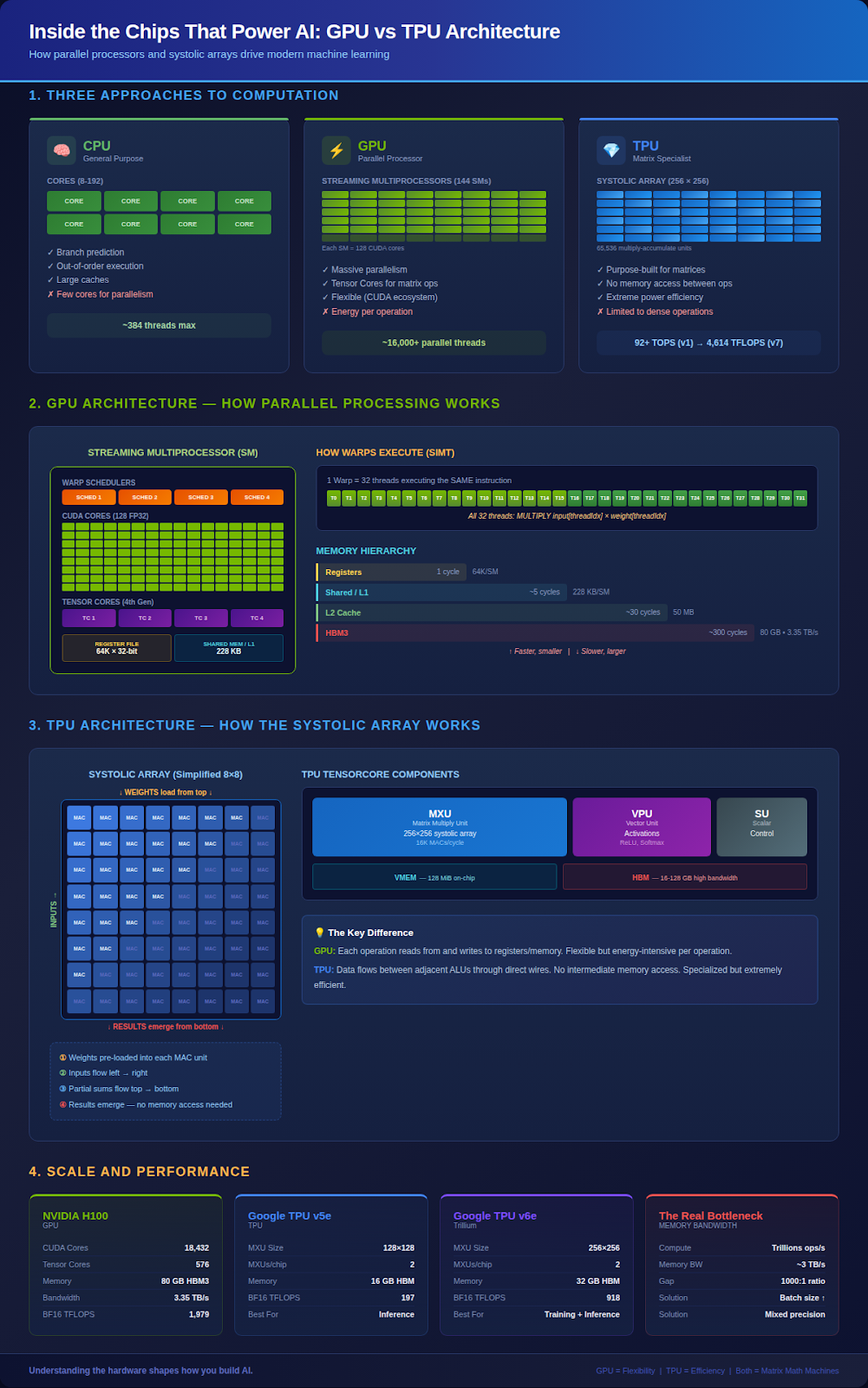
A CPU is a general-purpose processor. It’s brilliant at handling complex, sequential logic — branching, conditional execution, running your operating system, managing a thousand different processes at once. It has sophisticated features like branch prediction, out-of-order execution, and large caches that make individual operations incredibly fast.
But here’s the trade-off: all that sophistication takes up space on the chip. A modern CPU might have 8 to 192 cores. Each core is powerful, but there are relatively few of them. When you need to multiply two massive matrices together, a CPU has to crunch through it one small piece at a time.
Think of a CPU as a brilliant professor who can solve any problem you throw at them, but can only work on one problem at a time. For AI workloads, you don’t need a brilliant professor — you need ten thousand students who can each do simple multiplication simultaneously.
Inside a GPU
This is where GPUs come in, and the architecture is genuinely fascinating.
The Big Picture
A GPU is organized around units called Streaming Multiprocessors (SMs). If you think of a CPU as having a handful of powerful cores, an SM is a simpler, weaker processor — but a GPU has many of them.
NVIDIA’s H100, for example, has 144 Streaming Multiprocessors. Each SM contains 128 FP32 CUDA cores. That’s 18,432 cores total. Compare that to even the beefiest server CPU with its 192 cores.
But the number of cores alone doesn’t tell the full story. The magic of a GPU is in how it organizes and executes work.
Warps and Threads
GPUs don’t execute instructions one thread at a time. They group threads into bundles of 32 called “warps.” Every thread in a warp executes the same instruction at the same time, just on different data. This is called SIMT — Single Instruction, Multiple Threads.
For beginners: Imagine you have 32 students, and you say “everyone multiply your number by 5.” They all do it simultaneously. That’s a warp. Now imagine 144 classrooms, each with multiple groups of 32 students, all working at the same time. That’s a GPU.
For practitioners: This is why branch divergence kills GPU performance. If threads in a warp take different code paths (some go into the if, others into the else), the SM has to execute both paths sequentially, masking out threads that shouldn’t be active for each path. Your 32-wide parallelism just got cut in half or worse.
For architects: The SM’s warp schedulers can switch between warps in a single clock cycle — over 1000x faster than a CPU context switch. This is how GPUs hide memory latency. While one warp waits for data from memory, another warp that’s ready to compute takes over instantly. It’s not that the latency goes away; it’s that the GPU always has something else to do while waiting.
The Memory Hierarchy
This is where things get really interesting — and where a lot of performance optimization happens.
GPUs have a multi-level memory system:
- Registers: Fastest, closest to the cores. Each SM has 64K 32-bit registers.
- Shared Memory / L1 Cache: On-chip memory shared across threads in a block. The H100 gives you up to 228 KB per SM.
- L2 Cache: Larger, shared across the entire GPU. 50 MB on the H100.
- HBM (High Bandwidth Memory): The main GPU memory. 80 GB on the H100 with 3.35 TB/s bandwidth.
The gap between these levels is enormous. Reading from registers takes one clock cycle. Reading from HBM can take hundreds. The entire art of GPU optimization is keeping data as close to the compute units as possible.
Tensor Cores
Starting with the Volta architecture in 2017, NVIDIA added Tensor Cores — specialized hardware units designed specifically for matrix multiplication. A regular CUDA core does one floating-point operation per cycle. A Tensor Core can do an entire small matrix multiply (4x4) in a single operation.
This was NVIDIA’s acknowledgment that AI workloads were becoming their most important market. Rather than asking users to decompose matrix operations into individual multiplications, they built hardware that treats matrix multiplication as a primitive operation.
Inside a TPU
Google took a completely different approach. Instead of adapting a general-purpose parallel processor for AI (as NVIDIA did with GPUs), they designed a chip from scratch specifically for matrix multiplication.
The result is the Tensor Processing Unit, and its architecture is radically simple compared to a GPU.
The Systolic Array
The heart of a TPU is something called a systolic array. The name comes from the Greek word for “heart” — like a heartbeat, data pulses rhythmically through the processor in waves.
Here’s how it works.
Imagine a grid of 256 × 256 tiny processors — that’s 65,536 multiply-accumulate units arranged in a square. Each unit can do one thing: multiply two numbers and add the result to a running sum.
To perform a matrix multiplication:
- The weight matrix gets loaded into the grid — each unit holds one weight value
- Input values enter from the left side, one row at a time, flowing horizontally
- As an input value passes through each unit, the unit multiplies it by its stored weight and adds the result to a partial sum flowing down from above
- The final results emerge from the bottom of the array
For beginners: Think of it like an assembly line in a factory. You don’t have one worker doing every step of building a product. Instead, each worker does one small task and passes the item to the next person. By the time a product reaches the end of the line, it’s complete — and new products are continuously entering the line behind it.
For practitioners: The critical insight is that data flows through the array without going back to memory. In a GPU, every operation reads from and writes to registers. In a TPU’s systolic array, intermediate results pass directly between adjacent ALUs through wires. No register files, no memory access, no cache hierarchy for the matrix math itself. This is dramatically more power-efficient.
For architects: The trade-off is flexibility. A systolic array is extraordinary at dense matrix multiplication with predictable access patterns. It struggles with sparse matrices, conditional execution, and operations that need random memory access. TPUs are designed for one thing, and they do that one thing at extreme efficiency.
The Full Picture
A TPU chip contains one or more TensorCores (not to be confused with NVIDIA’s Tensor Cores — confusing, I know). Each TensorCore has:
- MXU (Matrix Multiply Unit): The systolic array itself — 128×128 on earlier versions, 256×256 on the latest TPU v6e
- VPU (Vector Processing Unit): Handles everything that isn’t matrix multiplication — activation functions, normalization, element-wise operations
- Scalar Unit: Control flow and address computation
- HBM: High Bandwidth Memory for storing tensors
- VMEM: On-chip vector memory, like a programmer-controlled L1 cache
The beauty of this architecture is its simplicity. Data flows from HBM into VMEM, from VMEM into the systolic array, results flow out. There’s no branch prediction, no speculative execution, no out-of-order processing. The chip does exactly what you tell it, in exactly the order you specify.
This deterministic execution model is why TPUs can deliver consistent latency that GPUs sometimes can’t match — there’s simply less that can go wrong or vary between runs.
GPU vs TPU: When Each One Wins
So which is better? The honest answer: it depends on what you’re doing.
GPUs excel when:
- You need flexibility — research, experimentation, varied workloads
- Your model involves significant non-matrix operations (custom kernels, sparse operations)
- You’re working with the CUDA ecosystem and its massive library of optimized software
- You need to run different types of workloads on the same hardware
TPUs excel when:
- Your workload is dominated by dense matrix multiplication (most transformer training and inference)
- You’re working at massive scale with homogeneous workloads
- Power efficiency matters — TPUs deliver significantly more operations per watt
- You’re in the Google Cloud ecosystem using JAX or TensorFlow
Here’s the interesting trend: these architectures are converging. NVIDIA keeps adding more specialized matrix hardware (Tensor Cores) to their GPUs, making them more TPU-like. Meanwhile, Google keeps adding more general-purpose capability to TPUs (SparseCores for irregular workloads, better vector units). The line between them is blurring.
Why Memory Bandwidth Is the Real Bottleneck
Here’s something that isn’t obvious until you’ve worked with this hardware: for most AI workloads, the bottleneck isn’t compute. It’s memory bandwidth.
Modern GPUs and TPUs can perform tens to hundreds of trillions of operations per second. But they can only read data from memory at a few terabytes per second. The math creates a gap — the processors can crunch numbers faster than they can be fed.
This is why you hear so much about:
- HBM (High Bandwidth Memory): Stacked memory modules physically close to the processor, providing much higher bandwidth than traditional DRAM
- Arithmetic intensity: The ratio of compute operations to memory accesses. Operations with high arithmetic intensity (like large matrix multiplications) are “compute-bound” and can keep the hardware busy. Operations with low arithmetic intensity (like element-wise additions) are “memory-bound” and leave expensive silicon sitting idle
- Batch size tuning: Larger batches mean larger matrices, which mean more computation per byte of data moved. This is why increasing batch size often improves hardware utilization
- Mixed precision: Using 16-bit or 8-bit numbers instead of 32-bit means you can move twice or four times as much data in the same bandwidth, and the compute units can process it proportionally faster
Understanding this relationship between compute and memory is, honestly, more practically useful than knowing the details of CUDA cores or systolic arrays. It’s the lens through which hardware decisions start making sense.
What This Means If You’re Building AI Systems
If you’re an engineer building or deploying AI systems, here’s what all of this translates to:
Model selection has hardware implications. Dense transformer models map beautifully to both GPUs and TPUs. Models with heavy sparse operations or complex control flow? GPUs handle those better.
Batch size isn’t just a hyperparameter. It directly affects how well you utilize the hardware. Tiny batch sizes leave most of your GPU/TPU’s compute units idle. This is especially true for TPUs, where the systolic array needs large enough matrices to fill the 128×128 or 256×256 grid.
Precision matters more than you think. Dropping from FP32 to BF16 doesn’t just halve memory usage — it can double throughput because you’re moving data twice as fast and the specialized hardware processes lower-precision operations at higher rates. Most modern training uses mixed precision for exactly this reason.
The software stack matters as much as the hardware. CUDA’s ecosystem is a genuine competitive moat for NVIDIA. The best hardware in the world is useless without optimized kernels and libraries. This is why NVIDIA maintains such a dominant position despite TPUs being architecturally superior for pure matrix multiplication.
Looking Forward
The race between GPU and TPU architectures is one of the most fascinating competitions in chip design right now.
NVIDIA is pushing toward more specialization — each generation adds more matrix-specific hardware and higher-bandwidth memory. Their Blackwell architecture took this further with dedicated transformer engines.
Google is pushing toward more flexibility — SparseCores for irregular workloads, larger systolic arrays, and better interconnects for scaling across thousands of chips.
And then there are the newcomers. AWS has Trainium, designed specifically for training large models. AMD has MI300X. Intel has Gaudi. Startups like Groq, Cerebras, and SambaNova are exploring radically different architectures.
The common thread? Everyone is trying to solve the same fundamental problem: move data less, multiply matrices faster, and use less power doing it.
Understanding the basics of how these chips work won’t make you a hardware engineer. But it’ll make you a significantly better AI engineer. When you know that a systolic array needs dense, predictable data, you understand why padding and batching matter. When you know that GPU performance depends on hiding memory latency with enough active warps, you understand why occupancy and memory access patterns are so critical.
The hardware shapes what’s possible. The more you understand it, the better you can use it.